今天我们来学习STM32的DAC模块与DMA控制器的配合使用。
一、DAC配置
STM32中的数字/模拟转换模块(DAC)是12位数字输入,0 ~ VREF+范围电压输出的DAC。其可以配置成8位或12位模式,也可以与DMA控制器配合使用。DAC工作在12位模式时,数据可以设置成左对齐或右对齐。DAC有2个输出通道,每个通道都有单独的转换器,可以工作在双DAC模式。在此模式下,可以同步的更新2个通道的输出,这2个通道的转换可以同时进行,也可以分别进行。
/**
  * @brief  使能DAC的时钟,初始化GPIO
  * @param  无
  * @retval 无
  */
static void DAC_Config(void)
{
  GPIO_InitTypeDef GPIO_InitStructure;
  DAC_InitTypeDef  DAC_InitStructure;
  /* 使能GPIOA时钟 */
  RCC_APB2PeriphClockCmd(RCC_APB2Periph_GPIOA, ENABLE);
/* 使能DAC时钟 */
  RCC_APB1PeriphClockCmd(RCC_APB1Periph_DAC, ENABLE);
  /* DAC的GPIO配置,模拟输入 */
  GPIO_InitStructure.GPIO_Pin =  GPIO_Pin_4 | GPIO_Pin_5;
  GPIO_InitStructure.GPIO_Mode = GPIO_Mode_AIN;// 为了避免寄生的干扰与额外的功耗,管脚PA4/PA5在使能之前应当设置为模拟输入
  GPIO_Init(GPIOA, &GPIO_InitStructure);
  DAC_InitStructure.DAC_Trigger = DAC_Trigger_T2_TRGO;//使用TIM2作为触发源
  DAC_InitStructure.DAC_WaveGeneration = DAC_WaveGeneration_None;//不使用波形发生器
  DAC_InitStructure.DAC_OutputBuffer = DAC_OutputBuffer_Disable;//不使用DAC输出缓冲
  /* 配置DAC 通道1 */
  DAC_Init(DAC_Channel_1, &DAC_InitStructure);
  /* 配置DAC 通道2 */
  DAC_Init(DAC_Channel_2, &DAC_InitStructure);
  /* 使能通道1 由PA4输出 */
  DAC_Cmd(DAC_Channel_1, ENABLE);

  /* 使能通道2 由PA5输出 */
  DAC_Cmd(DAC_Channel_2, ENABLE);

    /* 使能DAC1的DMA请求 */
    DAC_DMACmd(DAC_Channel_1, ENABLE);
  /* 使能DAC2的DMA请求 */
  DAC_DMACmd(DAC_Channel_2, ENABLE);
}STM32F103的DAC输出在PA4/5两个引脚,为了避免寄生的干扰与额外的功耗,在使能PA4/5的DAC复用功能之前,我们要把这两个引脚配置成“模拟输入”模式。
DAC_InitTypeDef DAC_InitStructure;
首先定义一个结构体DAC_InitStructure,其类型为DAC_InitTypeDef,其成员有4个,分别为:DAC触发器、波形生成、噪声或三角波幅度、输出缓冲。
/* 使能DAC时钟 */
  RCC_APB1PeriphClockCmd(RCC_APB1Periph_DAC, ENABLE);
DAC挂载于APB1总线上,使能其时钟。
  DAC_InitStructure.DAC_Trigger = DAC_Trigger_T2_TRGO;//使用TIM2作为触发源
  DAC_InitStructure.DAC_WaveGeneration = DAC_WaveGeneration_None;//不使用波形发生器
  DAC_InitStructure.DAC_OutputBuffer = DAC_OutputBuffer_Disable;//不使用DAC输出缓冲
  /* 配置DAC 通道1 */
  DAC_Init(DAC_Channel_1, &DAC_InitStructure);
DAC_Trigger_T2_TRGO、DAC_WaveGeneration_None、DAC_OutputBuffer_Disable分别被定义为:
#define DAC_Trigger_T2_TRGO                ((uint32_t)0x00000024) /*!< TIM2 TRGO selected as external conversion trigger for DAC channel */
#define DAC_WaveGeneration_None            ((uint32_t)0x00000000)
#define DAC_OutputBuffer_Disable           ((uint32_t)0x00000002)
DAC_Channel_1被定义为
#define DAC_Channel_1 ((uint32_t)0x00000000)
执行流来到DAC初始化库函数
  /* 配置DAC 通道1 */
  DAC_Init(DAC_Channel_1, &DAC_InitStructure);
DAC_Init();
/**
  * @brief  Initializes the DAC peripheral according to the specified
  *         parameters in the DAC_InitStruct.
  * @param  DAC_Channel: the selected DAC channel.
  *   This parameter can be one of the following values:
  *     @arg DAC_Channel_1: DAC Channel1 selected
  *     @arg DAC_Channel_2: DAC Channel2 selected
  * @param  DAC_InitStruct: pointer to a DAC_InitTypeDef structure that
  *        contains the configuration information for the specified DAC channel.
  * @retval None
  */
void DAC_Init(uint32_t DAC_Channel, DAC_InitTypeDef* DAC_InitStruct)
{
  uint32_t tmpreg1 = 0, tmpreg2 = 0;
  /* Check the DAC parameters */
  assert_param(IS_DAC_TRIGGER(DAC_InitStruct->DAC_Trigger));
  assert_param(IS_DAC_GENERATE_WAVE(DAC_InitStruct->DAC_WaveGeneration));
  assert_param(IS_DAC_LFSR_UNMASK_TRIANGLE_AMPLITUDE(DAC_InitStruct->DAC_LFSRUnmask_TriangleAmplitude));
  assert_param(IS_DAC_OUTPUT_BUFFER_STATE(DAC_InitStruct->DAC_OutputBuffer));
/*---------------------------- DAC CR Configuration --------------------------*/
  /* Get the DAC CR value */
  tmpreg1 = DAC->CR;
  /* Clear BOFFx, TENx, TSELx, WAVEx and MAMPx bits */
  tmpreg1 &= ~(CR_CLEAR_MASK << DAC_Channel);
  /* Configure for the selected DAC channel: buffer output, trigger, wave generation,
     mask/amplitude for wave generation */
  /* Set TSELx and TENx bits according to DAC_Trigger value */
  /* Set WAVEx bits according to DAC_WaveGeneration value */
  /* Set MAMPx bits according to DAC_LFSRUnmask_TriangleAmplitude value */
  /* Set BOFFx bit according to DAC_OutputBuffer value */
  tmpreg2 = (DAC_InitStruct->DAC_Trigger | DAC_InitStruct->DAC_WaveGeneration |
             DAC_InitStruct->DAC_LFSRUnmask_TriangleAmplitude | DAC_InitStruct->DAC_OutputBuffer);
  /* Calculate CR register value depending on DAC_Channel */
  tmpreg1 |= tmpreg2 << DAC_Channel;
  /* Write to DAC CR */
  DAC->CR = tmpreg1;
}
上面为函数定义,我们按照代码顺序一条条来对其进行分析。
tmpreg1 = DAC->CR;
tmpreg1 = 0;因为这个时候还没有配置CR寄存器,所以其值为0。
tmpreg1 &= ~(CR_CLEAR_MASK << DAC_Channel);
因为0与上任何数都为0,所以tmpreg1仍然是0。
  tmpreg2 = (DAC_InitStruct->DAC_Trigger | DAC_InitStruct->DAC_WaveGeneration |
             DAC_InitStruct->DAC_LFSRUnmask_TriangleAmplitude | DAC_InitStruct->DAC_OutputBuffer);
即tmpreg2 = (0x0000 0024 | 0x0000 0000 | 0 | 0x0000 0002) = 0x0000 0026;
tmpreg1 |= tmpreg2 << DAC_Channel;
即tmpreg1 = 0 | (0x0000 0026 << 0x0000 0000) = 0x0000 0026;
DAC->CR = tmpreg1;
即DAC->CR = 0x0000 0026,根据DAC控制寄存器描述

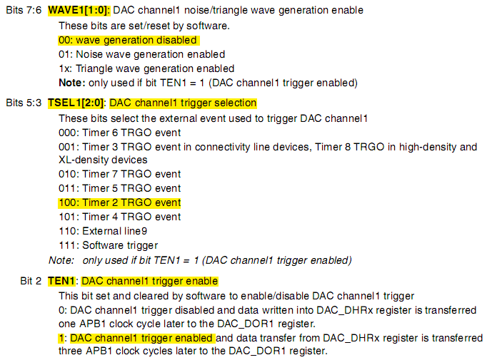
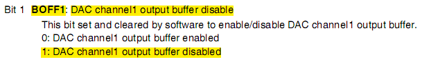
可知,此时DAC被配置为:波形生成不使能、定时器2更新事件被选为触发输出、DAC通道1输出缓冲不使能、使能DAC通道1触发器。
  /* 使能通道1 由PA4输出 */
  DAC_Cmd(DAC_Channel_1, ENABLE);
使能DAC通道1。
DAC_DMACmd(DAC_Channel_1, ENABLE);
根据DAC_DMACmd()函数定义
void DAC_DMACmd(uint32_t DAC_Channel, FunctionalState NewState)
{
  /* Check the parameters */
  assert_param(IS_DAC_CHANNEL(DAC_Channel));
  assert_param(IS_FUNCTIONAL_STATE(NewState));
  if (NewState != DISABLE)
  {
    /* Enable the selected DAC channel DMA request */
    DAC->CR |= (DAC_CR_DMAEN1 << DAC_Channel);
  }
  else
  {
    /* Disable the selected DAC channel DMA request */
    DAC->CR &= ~(DAC_CR_DMAEN1 << DAC_Channel);
  }
}
可得DAC->CR |= (DAC_CR_DMAEN1 << 0x0000 0000),DAC_CR_DMAEN1定义如下
#define DAC_CR_DMAEN1 ((uint32_t)0x00001000) /*!< DAC channel1 DMA enable */
所以DAC->CR |= (0x0000 1000 << 0x0000 0000)
即 DAC->CR |= 0x0000 1000,即DAC->CR寄存器的Bit12置1。
由寄存器的描述
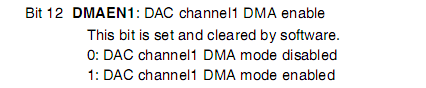
可知,此时DAC被配置为:DAC通道1的DMA模式被使能。
二、定时器配置
/**
  * @brief  配置TIM
  * @param  无
  * @retval 无
  */
static void DAC_TIM_Config(void)
{
TIM_TimeBaseInitTypeDef    TIM_TimeBaseStructure;
/* 使能TIM2时钟,TIM2CLK 为72M */
  RCC_APB1PeriphClockCmd(RCC_APB1Periph_TIM2, ENABLE);
  /* TIM2基本定时器配置 */
 // TIM_TimeBaseStructInit(&TIM_TimeBaseStructure);
  TIM_TimeBaseStructure.TIM_Period = 20;       //定时周期 20
  TIM_TimeBaseStructure.TIM_Prescaler = 0x0;       //预分频器为0
  TIM_TimeBaseStructure.TIM_ClockDivision = 0x0;    //时钟分频因子
  TIM_TimeBaseStructure.TIM_CounterMode = TIM_CounterMode_Up;  //向上计数模式
  TIM_TimeBaseInit(TIM2, &TIM_TimeBaseStructure);
  /* 配置TIM2触发源 */
  TIM_SelectOutputTrigger(TIM2, TIM_TRGOSource_Update);
/* 使能TIM2 */
  TIM_Cmd(TIM2, ENABLE);
}
有关定时器的配置之前已经有专门的文章描述过了,所以此处只做简单说明,具体描述请参照之前博文。
定时器2被配置为:开启定时器2时钟、设置时间周期值为20、预分频器值为0、分频因子为0、向上计数模式、并进行初始化。
TIM_SelectOutputTrigger(TIM2, TIM_TRGOSource_Update);
/**
  * @brief  Selects the TIMx Trigger Output Mode.
  * @param  TIMx: where x can be 1, 2, 3, 4, 5, 6, 7, 8, 9, 12 or 15 to select the TIM peripheral.
  * @param  TIM_TRGOSource: specifies the Trigger Output source.
  *   This paramter can be one of the following values:
  *
  *  - For all TIMx
  *     @arg TIM_TRGOSource_Reset:  The UG bit in the TIM_EGR register is used as the trigger output (TRGO).
  *     @arg TIM_TRGOSource_Enable: The Counter Enable CEN is used as the trigger output (TRGO).
  *     @arg TIM_TRGOSource_Update: The update event is selected as the trigger output (TRGO).
  *
  *  - For all TIMx except TIM6 and TIM7
  *     @arg TIM_TRGOSource_OC1: The trigger output sends a positive pulse when the CC1IF flag
  *                              is to be set, as soon as a capture or compare match occurs (TRGO).
  *     @arg TIM_TRGOSource_OC1Ref: OC1REF signal is used as the trigger output (TRGO).
  *     @arg TIM_TRGOSource_OC2Ref: OC2REF signal is used as the trigger output (TRGO).
  *     @arg TIM_TRGOSource_OC3Ref: OC3REF signal is used as the trigger output (TRGO).
  *     @arg TIM_TRGOSource_OC4Ref: OC4REF signal is used as the trigger output (TRGO).
  *
  * @retval None
  */
void TIM_SelectOutputTrigger(TIM_TypeDef* TIMx, uint16_t TIM_TRGOSource)
{
  /* Check the parameters */
  assert_param(IS_TIM_LIST7_PERIPH(TIMx));
  assert_param(IS_TIM_TRGO_SOURCE(TIM_TRGOSource));
  /* Reset the MMS Bits */
  TIMx->CR2 &= (uint16_t)~((uint16_t)TIM_CR2_MMS);
  /* Select the TRGO source */
  TIMx->CR2 |=  TIM_TRGOSource;
}
由上述触发源选择函数定义
TIM2->CR2 = 0 & (uint16_t)~((uint16_t)TIM_CR2_MMS) = 0;
由定时器2的控制寄存器2的描述

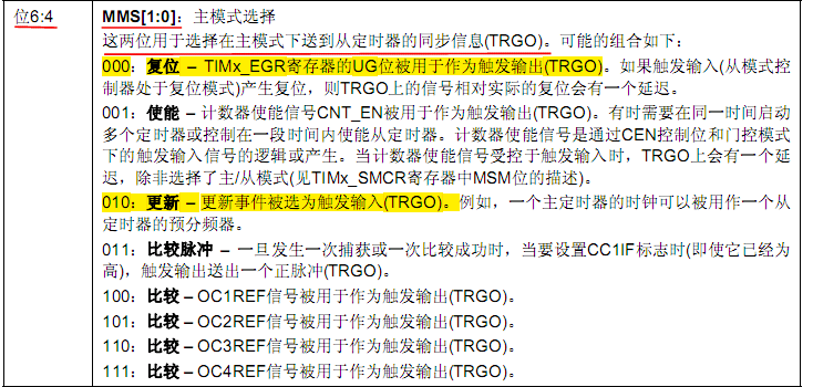
可知,定时器2被配置为:复位MMS位。
TIM2->CR2 |= TIM_TRGOSource;
TIM_TRGOSource_Update被定义为
#define TIM_TRGOSource_Update ((uint16_t)0x0020)
所以TIM2->CR2 = 0 | 0x0020 = 0x0020;
由定时器2的CR2寄存器描述可知
定时器2被配置为:定时器2的更新事件被选为触发输入(TRGO)。
三、DMA配置
STM32的DMA(直接存储器存取)用来提供外设与存储器或者存储器与存储器之间的高速数据传输。无须CPU任何干预,通过DMA,数据可以快速移动,这就节省了CPU的资源来做其他事情。STM32F103有两个DMA控制器,一共有12个通道(DMA1有7个,DMA2有5个),每个通道专门用来管理来自于一个或多个外设对存储器访问的请求。还有一个仲裁器用于协调各个DMA请求的优先权。
/**
  * @brief  配置DMA
  * @param  无
  * @retval 无
  */
static void DAC_DMA_Config(void)
{
DMA_InitTypeDef  DMA_InitStructure;
/* 使能DMA2时钟 */
RCC_AHBPeriphClockCmd(RCC_AHBPeriph_DMA2, ENABLE);
/* 配置DMA2 */
  DMA_InitStructure.DMA_PeripheralBaseAddr = DAC_DHR12RD_Address;//外设数据地址
  DMA_InitStructure.DMA_MemoryBaseAddr = (uint32_t)&DualSine12bit ;//内存数据地址 DualSine12bit
  DMA_InitStructure.DMA_DIR = DMA_DIR_PeripheralDST;//数据传输设置外设为目的地
  DMA_InitStructure.DMA_BufferSize = 32;//缓存大小为32位
  DMA_InitStructure.DMA_PeripheralInc = DMA_PeripheralInc_Disable;//外设数据地址固定
  DMA_InitStructure.DMA_MemoryInc = DMA_MemoryInc_Enable;//内存数据地址自增
  DMA_InitStructure.DMA_PeripheralDataSize = DMA_PeripheralDataSize_Word;//外设数据以字为单位
  DMA_InitStructure.DMA_MemoryDataSize = DMA_MemoryDataSize_Word;//内存数据以字为单位
  DMA_InitStructure.DMA_Mode = DMA_Mode_Circular;//循环模式
  DMA_InitStructure.DMA_Priority = DMA_Priority_High;//高DMA通道优先级
  DMA_InitStructure.DMA_M2M = DMA_M2M_Disable;//非内存至内存模式
  DMA_Init(DMA2_Channel4, &DMA_InitStructure);
  /* 使能DMA2-14通道 */
  DMA_Cmd(DMA2_Channel4, ENABLE);

  DMA_Init(DMA2_Channel3, &DMA_InitStructure);
  DMA_Cmd(DMA2_Channel3, ENABLE);
}
DMA_InitTypeDef DMA_InitStructure;
首先定义一个结构体DMA_InitStructure,类型为DMA_InitTypeDef,成员为:DMA外设基地址、DMA内存基地址、DMA方向、DMA数据传输数量、DMA外设地址自增选择、DMA内存地址自增选择、DMA外设数据大小、DMA内存数据大小、DMA模式。
RCC_AHBPeriphClockCmd(RCC_AHBPeriph_DMA2, ENABLE);
使能DMA2时钟,2个DMA控制器全部挂载于AHB总线上。
相关配置参数的定义汇总如下
#define DAC_DHR12RD_Address 0x40007420 //0x40007420
这个地址可查询用户手册得知,为DAC基地址加上对应寄存器偏移地址。
uint32_t DualSine12bit[32];
DualSine12bit为一个32个元素的数组,其地址做为内存基地址。
#define DMA_DIR_PeripheralDST              ((uint32_t)0x00000010)
#define DMA_PeripheralInc_Disable          ((uint32_t)0x00000000)
#define DMA_MemoryInc_Enable               ((uint32_t)0x00000080)
#define DMA_PeripheralDataSize_Word        ((uint32_t)0x00000200)
#define DMA_MemoryDataSize_Word            ((uint32_t)0x00000800)
#define DMA_Mode_Circular                  ((uint32_t)0x00000020)
#define DMA_Priority_High                  ((uint32_t)0x00002000)
#define DMA_M2M_Disable                    ((uint32_t)0x00000000)
下面分析DMA初始化库函数
DMA_Init();
/**
  * @brief  Initializes the DMAy Channelx according to the specified
  *         parameters in the DMA_InitStruct.
  * @param  DMAy_Channelx: where y can be 1 or 2 to select the DMA and
  *   x can be 1 to 7 for DMA1 and 1 to 5 for DMA2 to select the DMA Channel.
  * @param  DMA_InitStruct: pointer to a DMA_InitTypeDef structure that
  *         contains the configuration information for the specified DMA Channel.
  * @retval None
  */
void DMA_Init(DMA_Channel_TypeDef* DMAy_Channelx, DMA_InitTypeDef* DMA_InitStruct)
{
  uint32_t tmpreg = 0;
  /* Check the parameters */
  assert_param(IS_DMA_ALL_PERIPH(DMAy_Channelx));
  assert_param(IS_DMA_DIR(DMA_InitStruct->DMA_DIR));
  assert_param(IS_DMA_BUFFER_SIZE(DMA_InitStruct->DMA_BufferSize));
  assert_param(IS_DMA_PERIPHERAL_INC_STATE(DMA_InitStruct->DMA_PeripheralInc));
  assert_param(IS_DMA_MEMORY_INC_STATE(DMA_InitStruct->DMA_MemoryInc));
  assert_param(IS_DMA_PERIPHERAL_DATA_SIZE(DMA_InitStruct->DMA_PeripheralDataSize));
  assert_param(IS_DMA_MEMORY_DATA_SIZE(DMA_InitStruct->DMA_MemoryDataSize));
  assert_param(IS_DMA_MODE(DMA_InitStruct->DMA_Mode));
  assert_param(IS_DMA_PRIORITY(DMA_InitStruct->DMA_Priority));
  assert_param(IS_DMA_M2M_STATE(DMA_InitStruct->DMA_M2M));
/*--------------------------- DMAy Channelx CCR Configuration -----------------*/
  /* Get the DMAy_Channelx CCR value */
  tmpreg = DMAy_Channelx->CCR;
  /* Clear MEM2MEM, PL, MSIZE, PSIZE, MINC, PINC, CIRC and DIR bits */
  tmpreg &= CCR_CLEAR_Mask;
  /* Configure DMAy Channelx: data transfer, data size, priority level and mode */
  /* Set DIR bit according to DMA_DIR value */
  /* Set CIRC bit according to DMA_Mode value */
  /* Set PINC bit according to DMA_PeripheralInc value */
  /* Set MINC bit according to DMA_MemoryInc value */
  /* Set PSIZE bits according to DMA_PeripheralDataSize value */
  /* Set MSIZE bits according to DMA_MemoryDataSize value */
  /* Set PL bits according to DMA_Priority value */
  /* Set the MEM2MEM bit according to DMA_M2M value */
  tmpreg |= DMA_InitStruct->DMA_DIR | DMA_InitStruct->DMA_Mode |
            DMA_InitStruct->DMA_PeripheralInc | DMA_InitStruct->DMA_MemoryInc |
            DMA_InitStruct->DMA_PeripheralDataSize | DMA_InitStruct->DMA_MemoryDataSize |
            DMA_InitStruct->DMA_Priority | DMA_InitStruct->DMA_M2M;
  /* Write to DMAy Channelx CCR */
  DMAy_Channelx->CCR = tmpreg;
/*--------------------------- DMAy Channelx CNDTR Configuration ---------------*/
  /* Write to DMAy Channelx CNDTR */
  DMAy_Channelx->CNDTR = DMA_InitStruct->DMA_BufferSize;
/*--------------------------- DMAy Channelx CPAR Configuration ----------------*/
  /* Write to DMAy Channelx CPAR */
  DMAy_Channelx->CPAR = DMA_InitStruct->DMA_PeripheralBaseAddr;
/*--------------------------- DMAy Channelx CMAR Configuration ----------------*/
  /* Write to DMAy Channelx CMAR */
  DMAy_Channelx->CMAR = DMA_InitStruct->DMA_MemoryBaseAddr;
}
函数定义如上。
tmpreg = DMAy_Channelx->CCR;
即tmpreg = 0;
tmpreg &= CCR_CLEAR_Mask;
即tmpreg = 0 & CCR_CLEAR_Mask = 0;
  tmpreg |= DMA_InitStruct->DMA_DIR | DMA_InitStruct->DMA_Mode |
            DMA_InitStruct->DMA_PeripheralInc | DMA_InitStruct->DMA_MemoryInc |
            DMA_InitStruct->DMA_PeripheralDataSize | DMA_InitStruct->DMA_MemoryDataSize |
            DMA_InitStruct->DMA_Priority | DMA_InitStruct->DMA_M2M;
即tmpreg = 0 | 0x0000 0010 | 0x0000 0020 | 0x0000 0000 | 0x0000 0080 | 0x0000 0200 | 0x0000 0800 | 0x0000 2000 | 0x0000 0000 = 0x0000 2AB0;
DMAy_Channelx->CCR = tmpreg;
即DMA2_Channel4->CCR = 0x0000 2AB0;根据DMA2的CCR寄存器描述
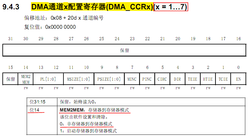
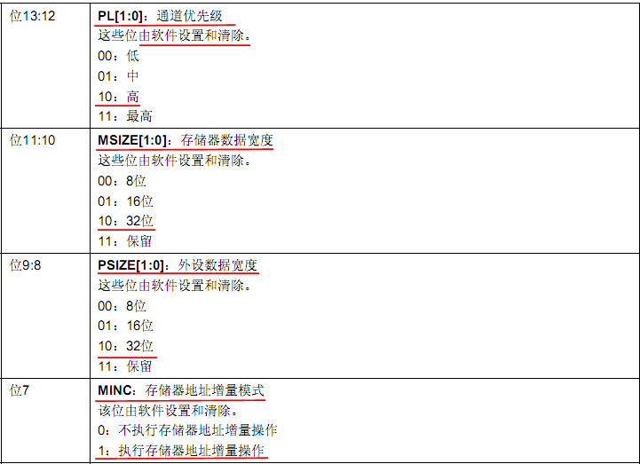
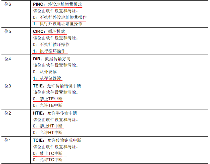
可知,DMA2被配置为:非存储器到存储器模式、通道优先级为高、存储器数据宽度为32位、外设数据宽度为32位、执行存储器地址增量操作、不执行外设地址增量操作、执行循环操作、从存储器读数据。
DMAy_Channelx->CNDTR = DMA_InitStruct->DMA_BufferSize;
即DMA2_Channel4->CNDTR = 32;由DMA2的CNDTR寄存器描述
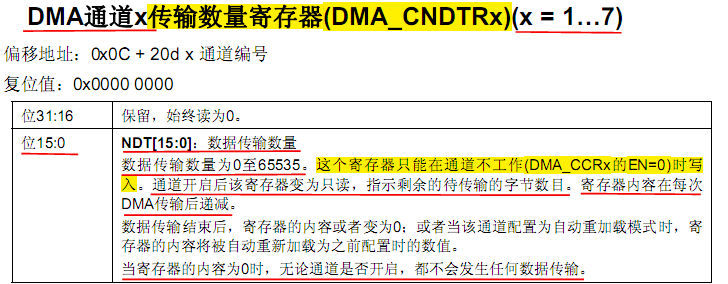
可知,DMA2被配置为:数据传输数量为32。
DMAy_Channelx->CPAR = DMA_InitStruct->DMA_PeripheralBaseAddr;
即DMA2_Channel4->CPAR = 0x40007420;由DMA2的CPAR寄存器描述
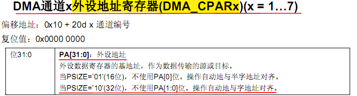
可知,DMA2被配置为:0x40007420(DAC_DHR12RD寄存器)为数据传输的目标地址,且操作自动地与字地址对齐。
DMAy_Channelx->CMAR = DMA_InitStruct->DMA_MemoryBaseAddr;
即DMA2_Channel4->CMAR = (uint32_t)&DualSine12bit;由DMA2的CMAR(内存地址寄存器)描述
可知,DMA2被配置为:DualSine12bit[]数组做为数据传输来源,且操作自动地与字地址对齐。
配置完毕,这样就可以以DMA的方式来使用STM32的DAC功能,通过改变代码中DMA数据源的数据就可以改变输出的电压值。
原创作品
